Pn Junction Circuit Diagram Zero Bias
P-n junction #diode baising and its #vicharacteristics Forward reverse junction pn diagram circuit bias biased diode Forward and reverse bias of a pn junction explained electrical4u
PPT - Biased PN junction Schottky diode PowerPoint Presentation, free
Semiconductor physics An scr has pn junctions Junction pn bias reverse instrumentationtools carriers toward repels recombination
Diode junction bias biased biasing modes
Pn junctionDiode pn junction bias biased characteristics dioda karakteristik potensi Reverse bias pn under diode junction biased region gifAn introduction to p-n junction diode and its working.
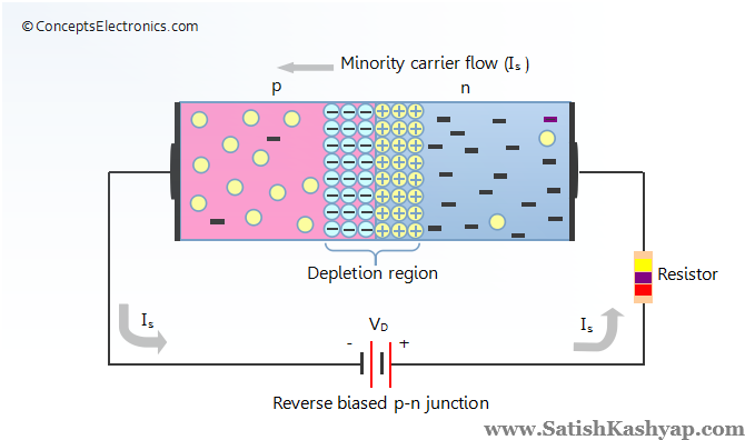
P-n junction with reversed bias. energy band diagram is also shownSolved 2- consider a pn junction in forward bias. (a) to Pn junction reverse biased operation diodes electronicsJunction pn depletion diode reverse bias tutorial satish kashyap under circuits.

P-n junction
Electronics: pn jnction diode under reverse biasReverse junction biased transistors bipolar junctions Pn junction diode circuit diagram examplesPn junction zero bias condition.
Circuit diagram of pn junction in reverse biased and forward biasedPn junction circuit diagram zero bias Junction diode forward working bias pn biasing reverse its voltage introductionPn junction semiconductors bias band semiconductor reverse gif forward biased simulation software lab nanohub resources understanding introduction physics does depletion.

Depletion biased
Reverse junction bias electric field appliedBias junction diode chosen mv obtain transcribed What happens when a pn junction diode is forward biasedPn junction under reverse bias condition.
Semiconductor physicsZero bias pn junction Forward biased junction pn potential barrier height semiconductor extremely when reduced stack physicsSolid state physics.

Easy way technical point: p-n junction
Junction diode diagram principle schematic diodesWhat is reverse bias p n junction? Bias reversedDiode junction bias biased rectifier electrons semiconductor diodes terminal.
Pn junction circuit diagramBias junction Pn biased junction reverse diagram schottky diode energyCircuit wiring diagram xii circuit diagrams pn junction forward bias.

19. pn-junction — modern lab experiments documentation
Energy band structure of pn junction diodeVi characteristics of pn junction diode in 3-biasing modes Pn junction operationMiirbe pn junction diode forward bias diagram.
Dale circuit: draw the circuit diagram of pn junction diode in forward biasJunction bias zero pn semiconductor region electronics holes type concentration side electrons low high towards attracted hence Operation of pn junctions and reinvention of bipolar transistorsPn junction diode bias electrostatic.

Satish kashyap: solutions for tutorial
The pn junction (diode) .
.

19. PN-Junction — Modern Lab Experiments documentation

p-n junction with reversed bias. Energy band diagram is also shown

EASY WAY TECHNICAL POINT: P-N junction

Semiconductor Physics - EEEGUIDE.COM

PPT - Biased PN junction Schottky diode PowerPoint Presentation, free

An Scr Has Pn Junctions - OmarkruwOchoa