P Channel Jfet Circuit Diagram
P-channel jfet basics Solved: for the p-channel jfet source-follower circuit in figur Jfet-junction field effect transistor,construction,symbol,operation
Solved: The p-channel JFET common-source amplifier in Figure P4.79
Jfet pinout Jfet transistor Baugewerbe n and p channel ff junction field effect transistor jfet
Jfet-junction field effect transistor,construction,symbol,operation
Jfet channel region curve fet transistor characteristics breakdown saturation ohmic cutoff transconductance voltage current idss resistor off depletion graph gateSolved: (a) draw the structure of a p-channel jfet similar to the Channel jfet circuit equivalent figureJfet channel voltage gate circuit dc.
N channel jfet circuit diagramP-channel jfet gate voltage – valuable tech notes Jfet amplifier figureJfet channel transistor effect field schematic symbols junction symbol diagram gate operation electronics source drain common configuration direction 2009 current.

Jfet channel transistor effect field junction type voltage jeft silicon
Jfet circuitJfet transistor polarity conventions effect field junction construction symbol operation Jfet circuit diagramJfet schematic symbols channel symbol transistor field junction effect electronics electrical circuit basics construction drain source choose board.
Jfet circuit diagramSolved: find the q-point for the p-channel jfet circuit in figu Channel effect field jfet transistors chapter pptJfet transistor.

Jfet channel circuit volts short open voltage example basics works positive transistors using
Characteristic jfet channel transfer drain electrical4u voltage current differ polarity applied direction case butJfet-junction field effect transistor Figure (a) p-channel jfet.Solved: the p-channel jfet common-source amplifier in figure p4.79.
Construction of p-channel junction field effect transistor (jfetNavy electricity and electronics training series (neets), module 21, 2 Field-effect transistors (fet)Jfet bias trazado posterior mediana circuitlab.

Jfet circuit applications figure operation source configuration input common
Junction field-effect transistors (jfet): operation, characteristicsNeets equivalent jfet circuit channel figure electricity electronics navy training series P-channel jfet characteristics curveJfet transistor biasing mosfet drain diferencia komponen bias fet rangkaian resistance junction transistors.
Jfet transistor mosfet drain comparisonJfet channel circuit construction effect field homemade transistors identical reversed regions counterpart except shown materials below type What is jfet: its construction, working and biasing techniquesStructure channel jfet draw similar.
Circuit diagram of p channel jfet
Jfet channel homofaciens abbildungJfet transistor: operation and characteristics – analyse a meter Figure 2-18.p-channel jfet equivalent circuitJfet channel chapter ppt powerpoint presentation characteristics structure slideserve.
Jfet transistor diagramJfet channel electrical figure junction What's the deal with phase reversal?Characteristic of junction field effect transistor.

Jfet or junction field effect transistor
N-channel jfet fixed bias with high gain = 200 .
.

jfet circuit diagram - IOT Wiring Diagram

Solved: Find the Q-point for the p-channel JFET circuit in Figu

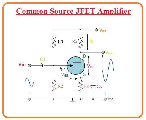
JFET

Solved: The p-channel JFET common-source amplifier in Figure P4.79

Solved: (a) Draw the structure of a p-channel JFET similar to the

Solved: For the p-channel JFET source-follower circuit in Figur